Semiconductors Made Easy: Just the Essentials
Semiconductors Made Easy: Just the Essentials is a B2B corporate training program that takes you from basic semiconductor principles to the global industry ecosystem in just 4 hours. In expert sessions led by John Kim, CEO of Nanum Consulting, you will cover semiconductor types and principles, manufacturing processes, and value chain analysis, so the complex structure of the industry becomes clear and easy to grasp. Organized into 4 core modules, the course is designed so that even non-engineers can pick up practical knowledge in a short time. Analysis of global semiconductor competition and the industry ecosystem also provides the insight needed to shape future business strategy. The curriculum draws on Nanum Consulting’s experience training 50+ major corporations and institutions.
💻 Start learning this topic with an online course →Who is this course for?
This course suits new hires who need a foundation in the semiconductor industry, employees moving into semiconductor-related roles from other departments, and planning, marketing, and sales staff who need to understand the semiconductor ecosystem. It is designed to be easy to follow without a technical background, so we recommend it for anyone in any role who wants to build a structured foundation in semiconductors.
What will you learn?
- Easily understand the basic principles and industry structure of semiconductors
Curriculum
- Conductors, insulators, and semiconductors explained simply
- Understanding vacuum tubes, transistors, and integrated circuits
- System semiconductors (CPU, GPU, AP, NPU, CIS, etc.)
- Memory semiconductors (RAM, ROM, flash memory, HBM, etc.)
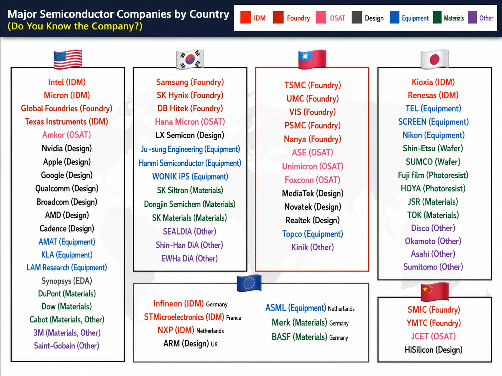
- Integrated device manufacturers (Samsung Electronics, Intel, SK hynix, Micron, etc.)
- Foundries (TSMC, Samsung Electronics, UMC, SMIC, GlobalFoundries, DB HiTek, etc.)
- Fabless (Qualcomm, NVIDIA, Apple (in-house design), AMD, MediaTek, etc.)
- OSAT (Amkor, ASE, JCET, SPIL, Hana Micron, Nepes, etc.)
- Wafer manufacturing (making the thin silicon disc on which circuits are etched)
- Oxidation, photolithography, and etching (insulate, pattern the circuit, and carve it in)
- Deposition, ion implantation, and metal interconnects (build the layers, tune the properties, lay the electrical paths)
- CMP, testing, and packaging (smoothing the surface, checking performance, and packing)
- Equipment (ASML, AMAT, LAM, TEL, EBARA, Hanmi Semiconductor, etc.)
- Materials (SUMCO, Siltronic, JSR, TOK, HOYA, AGC, etc.)
- Tools and consumables (3M, Disco, Saesol, Shinhan, Cabot, Fujimi, etc.)
- Trends in key countries (U.S., Taiwan, Korea, Japan, China, Europe)
Expected results / After the course
- A deeper understanding of technology-driven business
On-site training references
About the instructor

Start with an Online Course
Before you book on-site training, preview the essentials of this topic in an online course.
We tailor this course to your company
From diagnosis to execution — Nanum Consulting
FAQ

Semiconductors Made Easy: Just the Essentials
Semiconductors Made Easy: Just the Essentials is a B2B corporate training program that takes you from basic semiconductor principles to the global industry ecosystem in just 4 hours
- Easily understand the basic principles and industry structure of semiconductors
- A deeper understanding of technology-driven business
- Conductors, insulators, and semiconductors explained simply
- Understanding vacuum tubes, transistors, and integrated circuits
- System semiconductors (CPU, GPU, AP, NPU, CIS, etc.)
- Memory semiconductors (RAM, ROM, flash memory, HBM, etc.)
- Integrated device manufacturers (Samsung Electronics, Intel, SK hynix, Micron, etc.)
- Foundries (TSMC, Samsung Electronics, UMC, SMIC, GlobalFoundries, DB HiTek, etc.)
- Fabless (Qualcomm, NVIDIA, Apple (in-house design), AMD, MediaTek, etc.)
- OSAT (Amkor, ASE, JCET, SPIL, Hana Micron, Nepes, etc.)
- Wafer manufacturing (making the thin silicon disc on which circuits are etched)
- Oxidation, photolithography, and etching (insulate, pattern the circuit, and carve it in)
- Deposition, ion implantation, and metal interconnects (build the layers, tune the properties, lay the electrical paths)
- CMP, testing, and packaging (smoothing the surface, checking performance, and packing)
- Equipment (ASML, AMAT, LAM, TEL, EBARA, Hanmi Semiconductor, etc.)
- Materials (SUMCO, Siltronic, JSR, TOK, HOYA, AGC, etc.)
- Tools and consumables (3M, Disco, Saesol, Shinhan, Cabot, Fujimi, etc.)
- Trends in key countries (U.S., Taiwan, Korea, Japan, China, Europe)